- Home
- Solar Cell
Function of Solar Cells:
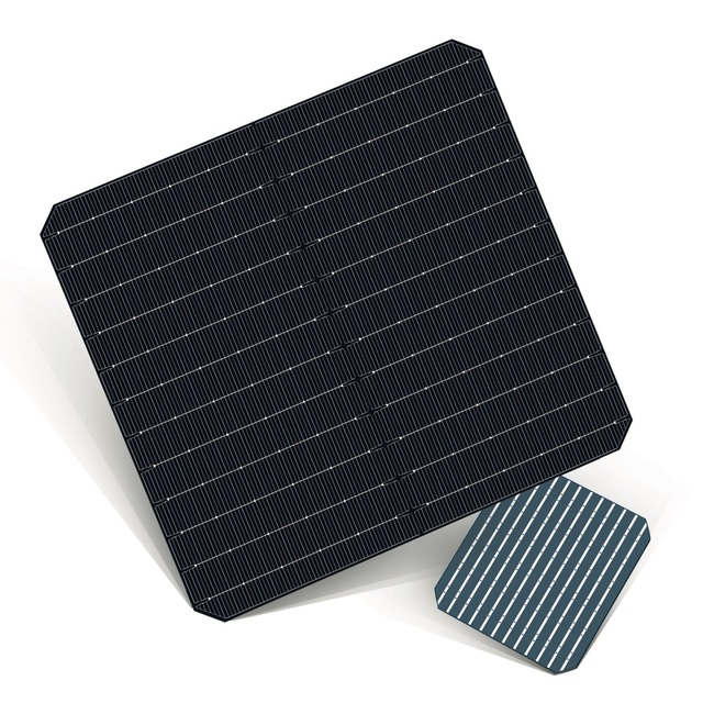
MONO PERC M2
Size: 156.75x156.75mm
Thinkness: 160μm±20μm
Front(-)5×0.7mm straight section barbus, Blue SiNx anti-reflecting coating
Back(+) Full aluminum cover on the back; 5×1.7mm segmented back electrode

MONO PERC G1
Size: 158.75x158.75mm
Thinkness: 160μm±20μm
Front(-)5×0.7mm straight section barbus, Blue SiNx anti-reflecting coating
Back(+) Full aluminum cover on the back; 5×1.7mm segmented back electrode 8

MONO PERC M6
Size: 166x166mm
Thinkness: 160μm±20μm
Front(-)9×0.08mm straight section barbus, Blue SiNx anti-reflecting coating
Back(+) 1.6mm±0.05mm aluminum busbar mosaic 6 segments and 1.7mm siliver pad

MONO PERC M10
Size: 182mm×182mmm(φ247mm)
Thinkness: 165μm±17.5μm
Front(-): Silicon oxide + blue silicon nitride compound anti-reflection coating(PID Free);Half- cut design;
Back(+) : Passivated layer (AlOx and SiNx) and Rear Contact (Al)

MONO PERC M12
Size: 210mm×210mmm(φ295mm)
Thinkness: 165μm±17.5μm
Front(-): Silicon oxide + blue silicon nitride compound anti-reflection coating(PID Free);Half- cut design;
Back(+) : Passivated layer (AlOx and SiNx) and Rear Contact (Al).

TOPCON M10
Size: 182.2×182.2±0.5mm(φ247mm±0.5mm)
Thinkness: 130μm±13μm
Front(-)16*0.05±0.035 mm
Back(+) 16*0.05±0.035 mm

TOPCON 210R
Size: 210mmX182mm±0.25mm, φ 272mm
Thinkness: 130μm±13μm
Front(-)16BB, 14pads, 168 fingers Barbus wide0.03±0.02 mm
Back(+) 16BB, 14pads, 192 fingers Barbus wide 0.03±0.02 mm

TOPCON M12
Size: 210mmX210mm±0.5mm , φ 295mm±0.5mm
Thinkness: 130μm±13μm
Front(-)18BB, 14pads, 168 fingers Barbus wide0.03±0.02 mm
Back(+) 18BB, 14pads, 192 fingers Barbus wide 0.03±0.02 mm
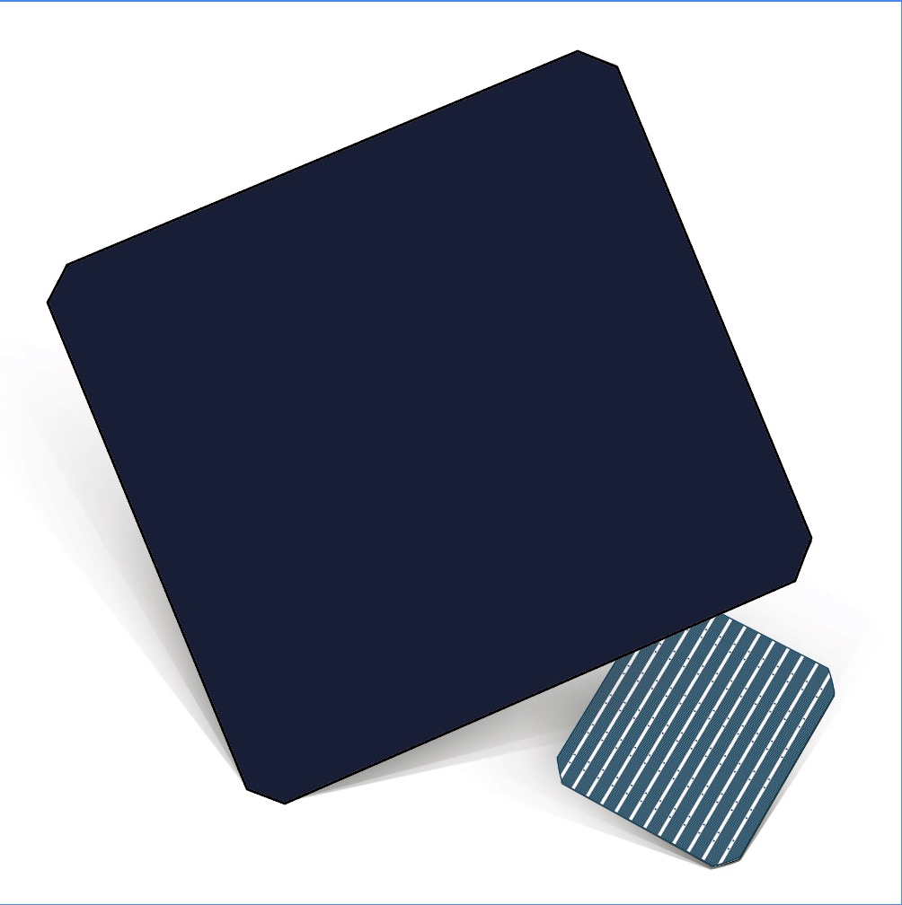
BC SOLAR CELL
Size: 182mmX182mm±0.5mm , φ 247mm±0.5mm
Thinkness: 130μm±13μm
Front(-)0BB
Back(+) 19BB, 14pads, 192 fingers Barbus wide 9.58±0.02 mm
REQUEST A QUOTE FOR MORE DETAILS
All You Need To Know About BC Solar Cells
What is the BC solar cells?
Key Features & Benefits of BC Solar cells!
By relocating all metal contacts to the rear side, BC solar cells eliminate front-side shading losses, allowing more photons to reach the silicon surface. This results in significantly higher energy conversion efficiency, surpassing conventional PERC and TOPCon technologies.
-Premium All-Black Appearance
The grid-free front surface creates a perfectly uniform, deep-black aesthetic. This clean and modern design makes BC cells especially attractive for high-end residential rooftops and architecturally demanding projects.
-Enhanced Energy Yield & Reliability
Improved light absorption translates into higher power output, while optimized rear-side interconnections reduce mechanical and thermal stress. The result is greater durability, long-term stability, and superior performance—even under partial shading conditions.
-Advanced Cell Architecture
BC technology is typically paired with N-type silicon substrates and advanced passivation methods such as IBC (Interdigitated Back Contact), delivering outstanding efficiency, low degradation, and long service life.
How many Type of BC Solar cells!
1. IBC (Interdigitated Back Contact)
The foundational back-contact cell design, featuring interdigitated metal fingers on the rear surface. By removing all front-side metallization, IBC cells achieve high efficiency and a clean, uniform appearance.
2. HPBC (Hybrid Passivated Back Contact)
A hybrid structure that combines IBC architecture with passivated contact concepts derived from TOPCon technology. Often implemented on P-type silicon substrates, HPBC offers a balance of high efficiency, cost competitiveness, and premium all-black aesthetics.
3. TBC (TOPCon Back Contact)
This design integrates TOPCon’s advanced passivation layers with a back-contact layout, typically using N-type silicon. TBC cells deliver excellent efficiency potential, low degradation, and strong scalability for mass production.
4. HBC (Heterojunction Back Contact)
The most advanced BC variant, merging heterojunction (HJT) technology with a back-contact structure. By utilizing thin amorphous silicon layers for superior surface passivation, HBC cells offer the highest theoretical efficiency potential, representing the cutting edge of photovoltaic cell development.
In summary, IBC forms the core back-contact concept, while HPBC, TBC, and HBC represent evolutionary hybrid designs that combine BC architecture with TOPCon or HJT technologies to push efficiency and performance to new levels.
How to reduce BC cell production costs?
1. Silver Consumption
According to PV Infolink data, current BC cells consume approximately 13 mg/W of silver, which is 2–3 mg/W higher than that of TOPCon cells. Looking ahead, the adoption of advanced rear-side metallization technologies such as OBB (One Busbar / Optical Busbar) structures is expected to significantly reduce silver consumption in BC cells.
2. Production Yield
In addition, the crossed rear-electrode layout necessitates corresponding adjustments in solder ribbon design, interconnection, and module packaging processes, which further impacts overall yield. Currently, mainstream TOPCon manufacturers have achieved cell yields exceeding 99%, while BC cell yields remain at approximately 95%.
3. Equipment Investment
As a result, the current capital expenditure for BC cell production lines remains relatively high, with CAPEX of approximately RMB 300 million per GW, exceeding that of TOPCon production lines.