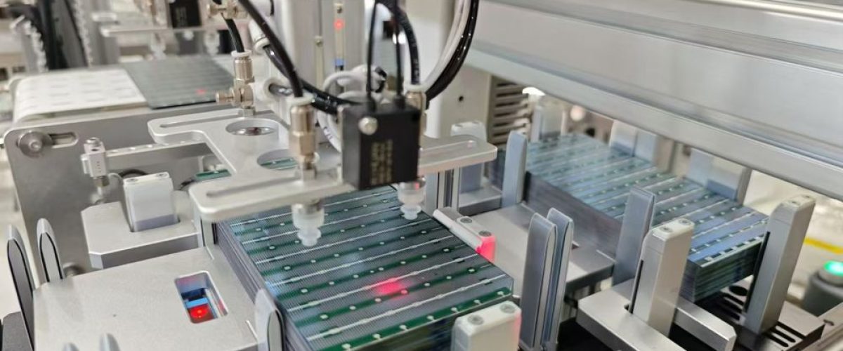
A standard module contains well over ten thousand solder joints. Each one is made in one to two seconds, at a temperature high enough to melt solder and low enough not to damage a silicon wafer that is now thinner than a sheet of paper. A single cold joint, a single crack, and the damage shows up first on an electroluminescence image and later as power loss and a hot spot in the field.
This article is about the joint: how it forms, what the stringer actually does, why heating uniformity is so hard, and where the process is heading as cells get thinner and architectures move to zero-busbar.
How a solder joint forms
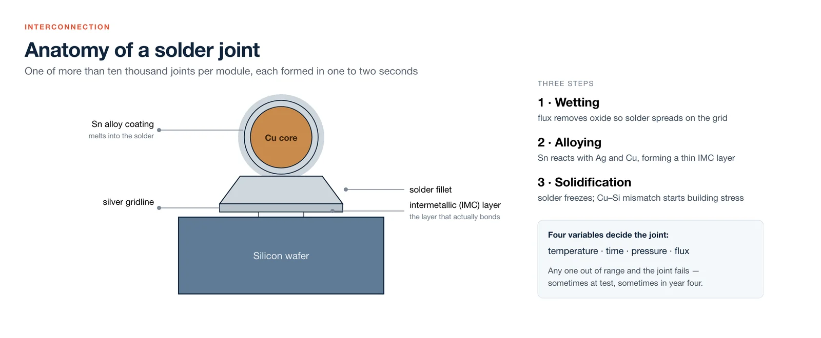
Soldering ribbon to a cell is a soft-soldering process. Heat melts the tin alloy coating on the ribbon; the molten solder wets the silver gridline on the cell; a metallurgical reaction takes place at the interface; cooling solidifies the joint.
That sequence breaks into three steps:
- Wetting. Flux first removes the oxide film from the ribbon coating and the silver gridline so the molten solder can spread. Poor wetting means the solder only rests on the grid — it looks joined but it is a cold joint.
- Alloying. Tin in the solder reacts with silver in the gridline and copper in the ribbon, forming a thin intermetallic compound (IMC) layer at the interface. That IMC is what actually bonds the two.
- Solidification. When heating stops, the solder freezes and the joint takes shape. The different contraction rates of copper and silicon start building stress immediately.
Four variables decide joint quality: temperature, time, pressure and flux. Temperature and time determine whether the solder melts fully and the IMC grows correctly. Pressure keeps ribbon and grid in intimate contact. Flux enables wetting. Get any one of them wrong and the joint fails — sometimes immediately, sometimes in year four.
Inside the stringer
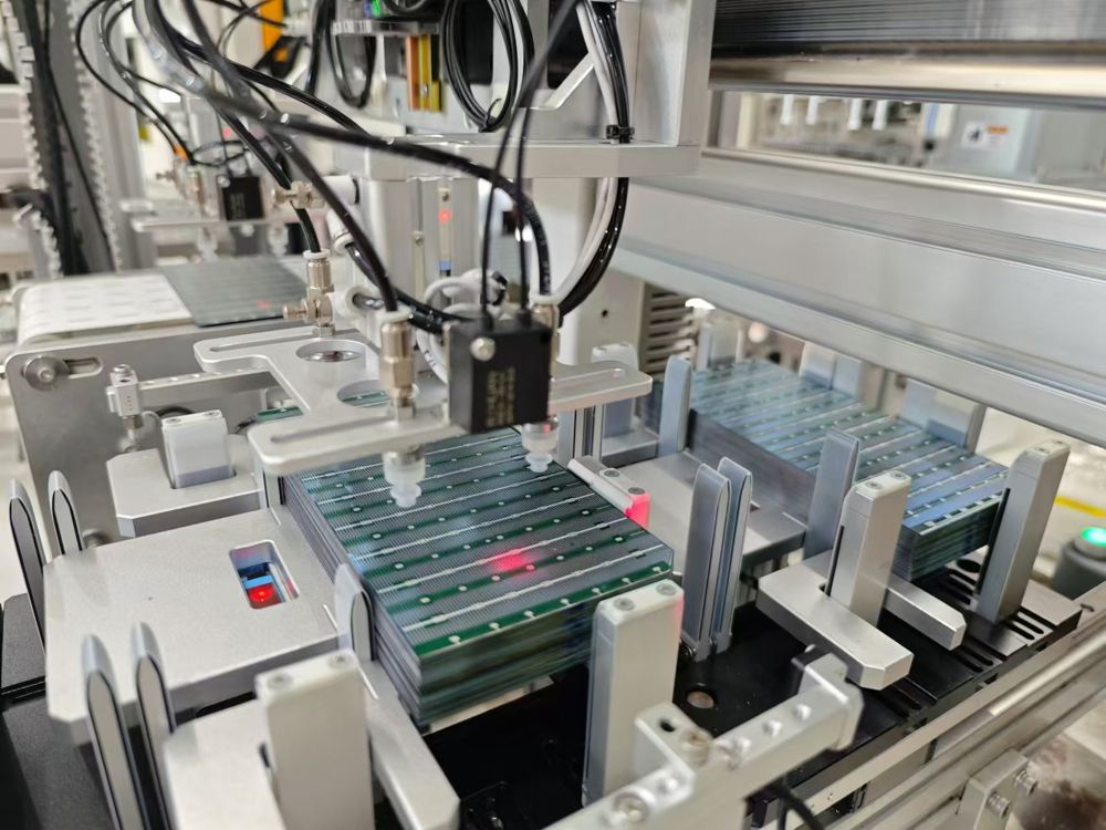
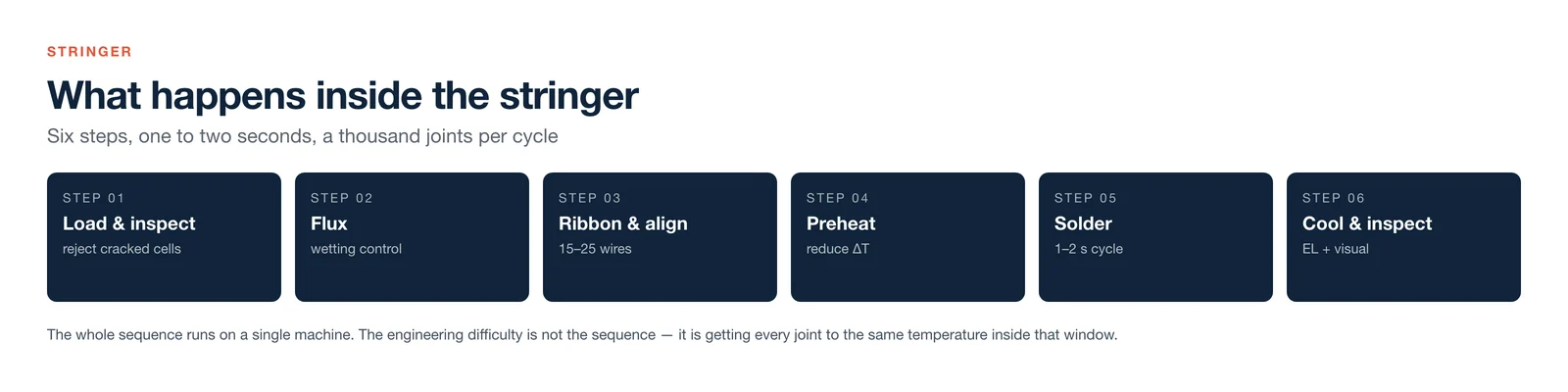
In a module factory, soldering happens on a stringer, which connects cells and ribbon one after another into a cell string. A typical sequence:
- Loading and inspection. Cells are loaded and checked visually or by EL so that already-cracked or chipped cells never enter the string.
- Flux application. Flux is applied to the ribbon or the cell's soldering pads. Too little gives poor wetting; too much leaves residue that affects appearance and long-term reliability.
- Ribbon placement and cell alignment. Ribbon is cut to length, straightened and aligned to the cell. With 15 to 25 fine round wires, alignment accuracy directly decides whether the joint lands or misses.
- Preheat. Cells sit on a heated plate to reduce the instantaneous temperature difference during soldering and lower thermal shock.
- Soldering. Pressure pins or plates hold the ribbon down while heat is applied quickly to melt the coating. This is the core step.
- Cooling and inspection. After the joints freeze, the string goes through EL and visual inspection before layup and busbar soldering.
The whole cycle is often one to two seconds. Getting a thousand joints to the right temperature in that window, uniformly, is the central engineering problem of the stringer.
How the heat gets there
| Method | Principle | Advantages | Watch out for |
|---|---|---|---|
| Infrared | Radiant heating from IR lamps | Non-contact, fast, mature technology | Uniformity depends on lamp layout and shadowing |
| Induction | Coil heats the ribbon itself | Heat concentrated in the ribbon; less heating of the cell | Sensitive to ribbon material and position; demanding setup |
| Hot air | Convection | Uniform temperature, low thermal shock | Slower |
| Laser | Local laser illumination of the joint | Precise area, small heat-affected zone | High equipment cost; hard to heat many joints at once |
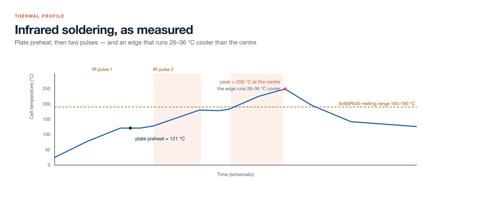
Infrared dominates installed capacity. What that looks like in practice is well documented: a 2025 study by Fraunhofer ISE modelled infrared soldering on an industrial stringer and validated the cell-temperature curve with thermocouples. The profile has two stages. The heated plate brings the cell to about 121 °C, then two IR pulses of roughly 1.2 seconds each lift it to about 180 °C and then to a peak near 250 °C.
The same data shows the weakness. The cell edge runs 26–36 °C cooler than the centre, because IR intensity falls off toward the edges and because the pressure tooling shadows and reflects light. Dropping lamp power from 70% to 50% narrows the centre-to-edge difference from about 36 °C to 26 °C and lowers the peak from roughly 249 °C to 219 °C.
The practical consequence: to get the edge joints to wet properly, the centre is often overheated. On one cell you can have over-soldering and cold joints at the same time, plus a larger thermal gradient through the silicon. This is why stringer recipe development spends so much time comparing pull strength at centre and edge joints.
The temperature window: joint strength versus cell damage
Why not simply raise the temperature until every joint is good? Because the joint is a mechanical trap.
Copper expands at about 17 × 10⁻⁶/K, silicon at about 2.6 × 10⁻⁶/K. When the solder solidifies, ribbon and cell are locked together. As the assembly cools to room temperature, copper contracts far more than silicon, and the difference becomes thermal-mismatch strain.
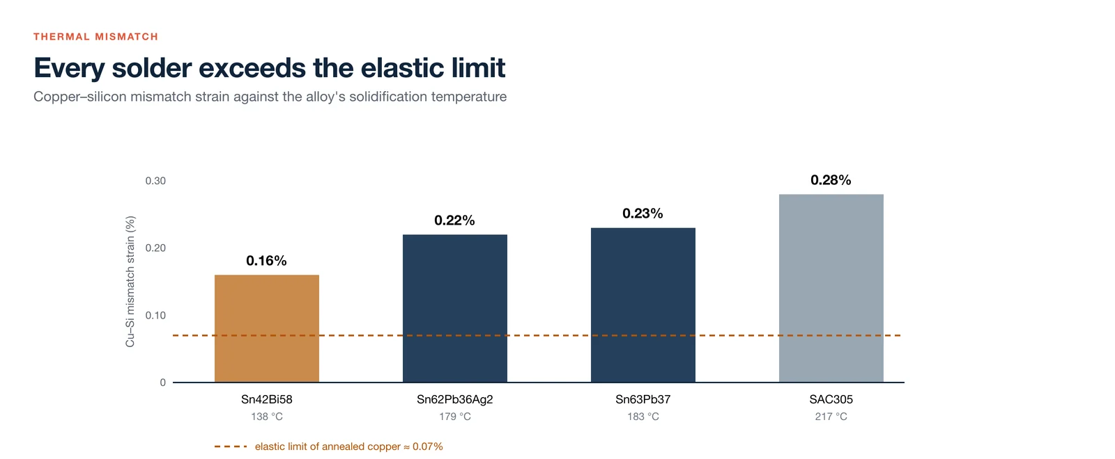
For the common tin-lead solder that solidifies at 183 °C, cooling to 25 °C produces roughly 0.23% mismatch strain. Annealed copper's elastic limit is only about 0.07%. The mismatch is more than three times the elastic range, so the copper ribbon must yield plastically during cooling. That is a design feature, not a defect: a soft ribbon absorbs the stress by deforming itself instead of pulling on the cell.
The consequence is important. Because the ribbon always yields, the stress left on the cell is governed mainly by the ribbon's yield strength, not linearly by the soldering temperature. Lower-melting solders reduce the mismatch — tin-bismuth at 138 °C gives about 0.16%, roughly 30% less than tin-lead — while SAC305 at 217 °C gives about 0.28%. Higher peak temperatures and worse uniformity also increase transient gradients and bowing.
But temperature cannot simply be lowered. Too little heat produces cold joints: incomplete wetting, poor IMC formation, low pull strength, and joints that crack under thermal cycling. The process window is the safe band between cold joints and microcracks — and it narrows every time the cell gets thinner or the ribbon finer.
Low-temperature interconnection for HJT
For heterojunction cells, temperature is a hard constraint. The amorphous-silicon passivation layer and the transparent conductive oxide are heat-sensitive, and process temperatures are generally kept below about 200 °C to avoid degrading passivation and conductivity. Conventional tin-lead profiles exceed that, so HJT needs dedicated low-temperature interconnection:
- Low-melt ribbon with tin-bismuth coatings. The difficulty is that bismuth is brittle, so fatigue performance has to be proven by thermal cycling.
- Conductive adhesive, using silver-filled adhesive instead of solder, cured at room or low temperature. Low stress, but higher material cost and a need to verify conductivity and long-term adhesion.
- Busbar-less interconnection, where ribbon is bonded with adhesive film and the joint forms during lamination. This is the 0BB route below.
Low-temperature processing is no longer an HJT-only concern. As cells thin, TOPCon and BC also face bowing and cracking pressure. TaiyangNews has reported that at a mainstream soldering temperature around 240 °C, BC cells tend to bow after stringing — which is one reason tape-based and adhesive interconnection routes are being developed.
0BB: moving the joint into the laminator
Zero-busbar is the biggest change in interconnection in years. The cell no longer carries printed busbars; ribbon is laid directly on the fine fingers. Critically, the electrical connection is often not made on the stringer at all but during lamination. The stringer's job becomes placing and fixing the ribbon in the right position.
| Route | Method | Advantages | Challenges |
|---|---|---|---|
| Solder plus dispensing | Ribbon soldered to the cell, then fixed with adhesive or tape | Strong bond, reworkable, uses existing equipment | Demanding soldering, precise dispensing, lower speed |
| Dispense plus lamination alloying | UV or hot-melt adhesive applied, ribbon pressed on, alloying completed in lamination | Removes the soldering step; wider process window | Requires protective film; defects only appear after lamination |
| One-piece film | Encapsulant, cells and ribbon laminated in one step, no flux | High adhesion, low risk of finger lift-off | Special film and rework equipment; defects detected late |
0BB also changes what is required of the ribbon itself:
- Coating melting point must match the lamination window, because the connection forms there. Low-melt coatings are preferred.
- Finer and more consistent wire — with no busbar to catch errors, diameter and straightness deviation turns directly into poor contact.
- Compatibility with film and adhesive, since coating, encapsulant and adhesive all act at once during lamination and must be validated together.
The last consequence is organisational: quality inspection moves downstream. With conventional stringing, EL after soldering catches most joint problems. With 0BB, some defects only appear after lamination — by which point the whole module is scrap. Front-end process stability matters more than ever.
Troubleshooting guide
| Symptom | Likely cause | Where to look |
|---|---|---|
| Cold joint, low pull strength | Insufficient temperature or flux; oxidised or thin coating | Heating power and time, flux, ribbon storage, coating thickness |
| Over-soldering, yellow joints | Too hot or too long | Reduce power or shorten dwell; check temperature uniformity |
| Microcracks, breakage | Ribbon yield strength too high, uneven temperature, excess pressure | Verify ribbon yield strength; improve preheat and uniformity; check tooling pressure |
| Misalignment, exposed pad | Ribbon camber, alignment error | Check straightness and side camber; recalibrate alignment |
| Solder balls, overflow | Coating too thick, temperature too high | Verify coating thickness; adjust profile |
| String bowing | Thermal-mismatch stress, ribbon too stiff | Lower soldering temperature; use softer ribbon; optimise cooling |
Many soldering problems do not originate in the stringer at all. They come from the ribbon: yield strength, coating thickness, straightness, storage condition. Soldering is where every property of the ribbon is finally tested.
The direction of travel
A reliable joint is the combined result of ribbon, cell, flux, equipment and recipe. From conventional stringing to 0BB, the form keeps changing but the contradiction does not: the joint must be strong without damaging the cell. The industry's answer is consistent — lower temperature, more concentrated heat, and connection later in the process, so that ever-thinner cells can be joined without being hurt.
The same problem on ZOEAST PV's lines
Everything above plays out daily on the two automatic module lines in Yixing. Stringer recipes are set per cell batch, not per product family: pull strength is checked at both centre and edge joints each shift, EL inspection follows stringing, and AOI runs on the cell line before lamination.
Ribbon is specified by yield strength, coating thickness, straightness and storage condition — the four properties that cause most soldering defects — and incoming coils are checked against those limits rather than against a generic diameter. As cells move below 130 µm, we shift to softer ribbon and lower peak temperature rather than pushing the process window.
Our project references show what comes off those lines; contact the engineering team if you want to audit the process before ordering.
Calculation notes: thermal-mismatch strain is estimated as ε = (αCu − αSi) × (Tsolidus − 25 °C), with αCu = 17 × 10⁻⁶/K and αSi = 2.6 × 10⁻⁶/K. Sn63Pb37 (183 °C) gives about 0.23%, Sn42Bi58 (138 °C) about 0.16%, SAC305 (217 °C) about 0.28%. The elastic strain limit of annealed copper is estimated from Rp0.2 ≈ 80 MPa and E ≈ 110 GPa, giving about 0.07%. These are one-dimensional approximations for illustration, excluding joint geometry, solder creep, cell thickness and temperature distribution. The infrared profile data follows the benchmark case in Joseph et al., "Simulation of infrared soldering of solar cells in an industrial stringer", EPJ Photovoltaics 16, 9 (2025).
Figures: ZOEAST PV, redrawn in English from the original technical article.