A 40 nm logic chip carries more than a dozen deposited films between the substrate and the final passivation layer: silicon oxide, silicon nitride, polysilicon, metals, high-k dielectrics. Each one has its own thickness, density, stress and conformality requirement. Almost all of them are made by just four processes: APCVD, LPCVD, PECVD and ALD.
Rank those four by how "advanced" they sound and you get ALD > PECVD > LPCVD > APCVD. Rank them by how much film they actually deposit on a 40 nm production line and the order roughly reverses: the two "oldest" techniques carry most of the layers, while the most advanced is used only in a handful of critical places.
That is not conservatism. Thin-film deposition is never a matter of picking the best technique. It is solving an equation with four constraints: thermal budget, film quality, structural complexity and throughput cost.

Three variables define all four techniques
- Where the energy comes from — pure heat, or a plasma? This sets the minimum temperature.
- Where the reaction happens — in the gas phase, or on the wafer surface? This sets uniformity and conformality.
- How thickness is controlled — by time (continuous deposition), or by chemical saturation (self-limiting cycles)? This sets precision and throughput.
Everything that follows is a consequence of those three choices.
The device cross-section: what each film is solving
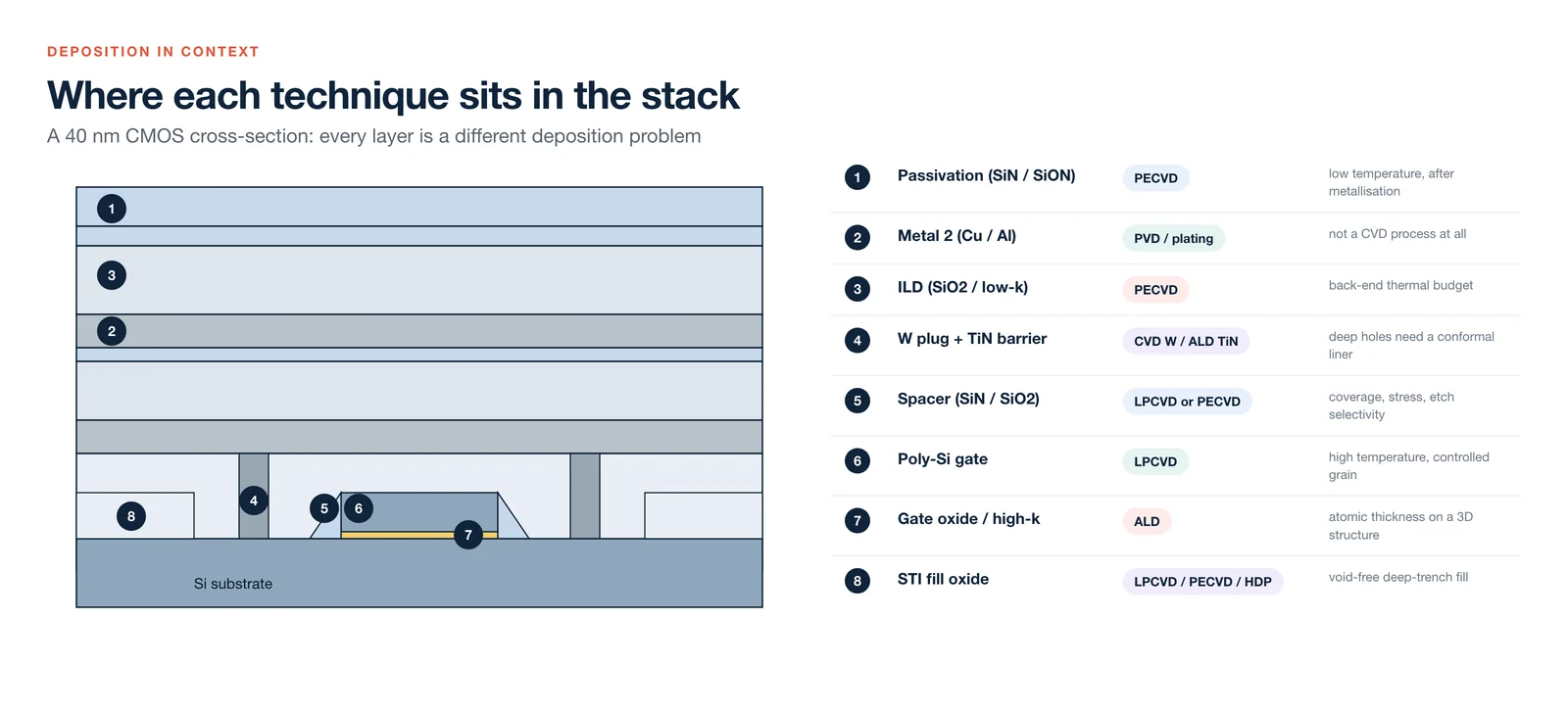
Take a 40 nm MOS transistor apart and the stack explains the tool choice:
- STI isolation — oxide filling shallow trenches between devices. Needs void-free fill, high density, controlled stress.
- Gate stack — gate oxide or high-k plus polysilicon or metal gate. Needs atomic-level thickness control and an excellent interface.
- Spacers — nitride or oxide beside the gate. Needs good coverage, etch resistance and controlled stress.
- Contacts and barriers — tungsten plugs with TiN/TaN liners. Needs uniform sidewall coverage in deep holes.
- ILD — dielectric between metal layers. Needs a low dielectric constant and void-free gap fill.
- Metal interconnect — copper or aluminium.
- Passivation — the top nitride that protects against moisture and mechanical damage.
| Film family | Typical materials | Core function | Key metrics |
|---|---|---|---|
| Oxide | SiO₂, PSG, BPSG | Insulation, isolation, ILD | Density, dielectric constant, gap fill |
| Nitride | SiN, SiON | Diffusion barrier, stress control, protection | Stress, density, barrier performance |
| Polysilicon | Poly-Si, a-Si | Gate material, resistors, sacrificial layers | Grain structure, doping, thickness uniformity |
| High-k / metal | HfO₂, Al₂O₃, TiN | Advanced gate stacks, metal barriers | Thickness precision, interface quality, conformality |
APCVD: fast, cheap, and rough
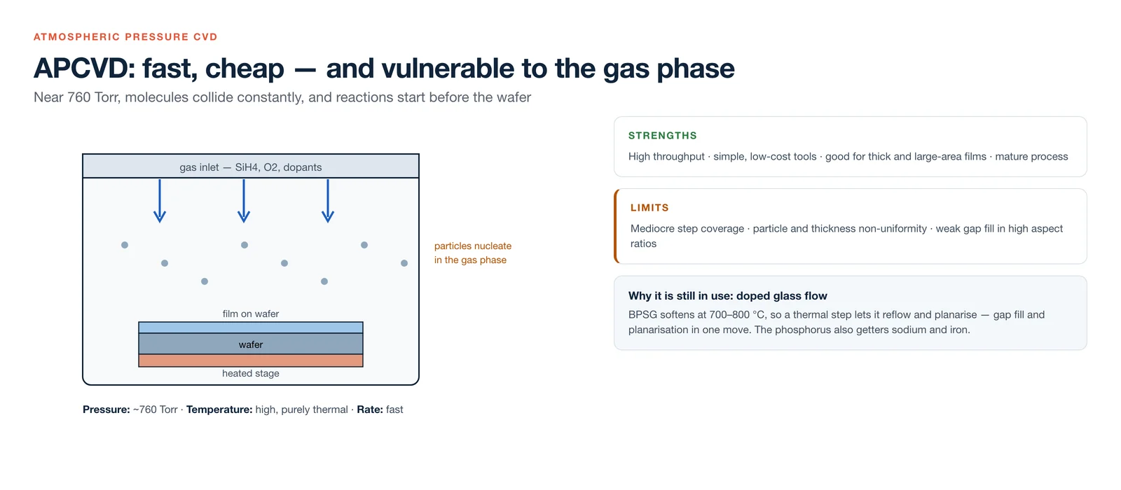
Atmospheric pressure CVD operates near 760 Torr. High gas density means fast mass transport and therefore high deposition rates — but it also means vigorous gas-phase reactions. Precursor molecules react with each other in mid-air before reaching the wafer, nucleate particles, and drop them onto the surface as contamination.
That is APCVD's central contradiction: to go fast you need high pressure and temperature, and going fast makes gas-phase reaction impossible to suppress.
| Advantages | Limitations |
|---|---|
| High throughput | Mediocre step coverage |
| Simple, low-cost equipment | Particle and thickness non-uniformity from gas-phase reaction |
| Good for thick and large-area films | Limited gap-fill capability |
| Mature process, proven in volume | Not the choice for high-aspect-ratio structures |
So why is it still in use? Doped glass flow. PSG and BPSG deposited by APCVD contain phosphorus and boron, which sharply lower the glass softening temperature. Plain SiO₂ needs well over 1,000 °C to flow; BPSG becomes mobile at 700–800 °C. After deposition, a thermal step lets the glass reflow like a liquid, filling steps and gaps and planarising the surface. Before CMP became universal, this was the main planarisation method, and it still solves two problems — gap fill and planarisation — in a single step.
Phosphorus also getters: it captures sodium, iron and other metal ions before they can migrate into the gate oxide. In reliability-critical processes, PSG doubles as contamination protection.
LPCVD: quality, purchased with temperature
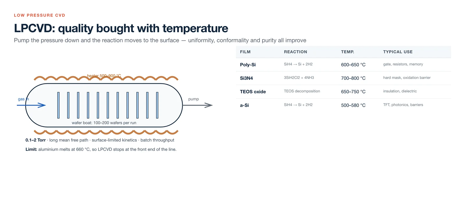
Drop the pressure to 0.1–2 Torr and the gas becomes rarefied, the mean free path lengthens, molecule collisions fall, and gas-phase reaction is suppressed. Deposition moves to the wafer surface: molecules adsorb, then react. Because the process is surface-controlled:
- Thickness uniformity improves — surface reaction rate is less sensitive to gas concentration.
- Conformality improves — molecules can diffuse to the bottom of a trench before reacting.
- Particles drop, because there is little gas-phase nucleation.
The workhorse is a horizontal tube furnace: a quartz tube, a surrounding heater, and a wafer boat holding 100–200 wafers per run. Batch processing is the throughput advantage — the per-wafer rate is not the fastest, but 150 wafers at a time adds up.
| Film | Typical reaction | Temperature | Use |
|---|---|---|---|
| Poly-Si | SiH₄ → Si + 2H₂ | 600–650 °C | Gate electrodes, resistors, memory structures |
| Si₃N₄ | 3SiH₂Cl₂ + 4NH₃ → Si₃N₄ + 6HCl + 6H₂ | 700–800 °C | STI hard masks, oxidation barriers, stress films |
| TEOS oxide | Thermal decomposition of TEOS | 650–750 °C | Insulation and dielectric layers |
| a-Si | SiH₄ → Si + 2H₂ | 500–580 °C | Displays, optoelectronics, barriers |
The fatal limitation is temperature. Between 500 and 900 °C, LPCVD is fine before metallisation (front end). Once aluminium — melting point 660 °C — and copper are present, it is unusable. That is the dividing line: LPCVD for the front end, PECVD for the back end.
PECVD: plasma buys you low temperature
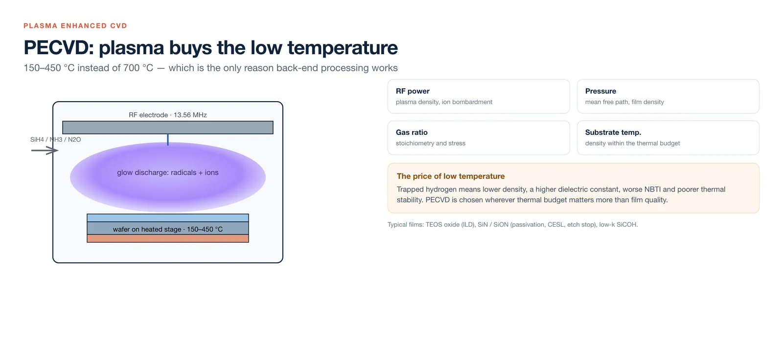
Thermal CVD supplies energy as heat, and heat destroys metals. PECVD replaces heat with a plasma. An RF supply, usually 13.56 MHz, strikes a glow discharge between electrodes; energetic electrons break gas molecules into radicals and ions that are chemically reactive enough to form films at 150–450 °C.
That single trade — 700 °C down to 300 °C — is the entire reason back-end processing exists.
Four parameters govern the result: RF power (plasma density and ion bombardment), pressure (mean free path, hence density and directionality), gas ratio (stoichiometry and stress), and substrate temperature (density, within the thermal budget).
The cost of low temperature is trapped hydrogen. At 150–450 °C, hydrogen does not have enough energy to desorb, so it stays in the film: SiN can contain 20–25 at% hydrogen, and SiO₂ several percent. The consequences are consistent:
- Lower film density, so moisture and ion barrier performance drops.
- Slightly higher dielectric constant than thermal oxide.
- NBTI degradation — hydrogen migrates to the gate-oxide interface under bias and temperature, creating interface states and shifting threshold voltage.
- Poor thermal stability: later high-temperature steps drive hydrogen out, shrinking the film and changing stress.
Everywhere PECVD is used, it is because thermal budget matters more than film quality. Typical applications: TEOS oxide for ILD and planarisation, SiN/SiON for passivation, stress control and etch stops, and low-k dielectrics such as SiCOH for interconnect isolation.
ALD: atomic control from self-limitation
Atomic layer deposition is the strangest of the four: absurdly slow, expensive, and indispensable in a few places.
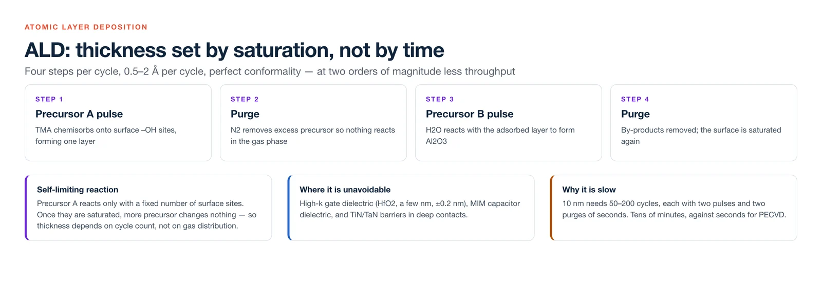
Instead of admitting two precursors together, ALD admits them one at a time, in a four-step cycle:
- Precursor A pulse — for example trimethylaluminium, which chemisorbs onto surface hydroxyl sites, forming a single layer.
- Purge — inert gas removes excess precursor A so it cannot react in the gas phase.
- Precursor B pulse — for example water, reacting with the adsorbed A to form Al₂O₃.
- Purge again — remove reactants and by-products.
Each cycle grows roughly 0.5–2 Å. Ten nanometres means repeating the cycle tens of times.
The key property is that step one is self-limiting: precursor A reacts only with surface sites, and the number of sites is fixed by surface chemistry, not by time. Once the sites are saturated, more precursor changes nothing. Thickness is therefore set by cycle count, not by time — which solves CVD's worst problem, thickness non-uniformity from gas distribution. Where gas reaches, the film grows equally. Conformality becomes essentially perfect, which is why ALD is irreplaceable in high-aspect-ratio structures, and it works at 100–400 °C, which matters for high-k metal gates.
The price is throughput. Ten nanometres requires 50–200 cycles, each with two pulses and two purges lasting seconds. That is tens of minutes, where PECVD deposits hundreds of nanometres in a few. Two orders of magnitude in productivity is why ALD is confined to critical layers: high-k gate dielectric, MIM capacitor dielectric, and thin metal barriers such as TiN and TaN.
The same SiO₂, four different results
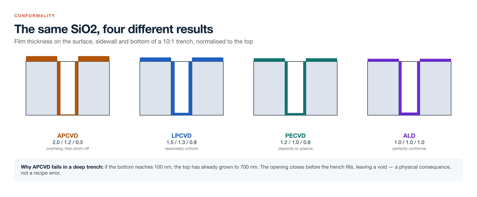
Deposit SiO₂ into a trench with a 10:1 aspect ratio using each technique, normalise the top thickness to 1, and measure:
| Technique | Top | Sidewall | Bottom | Behaviour |
|---|---|---|---|---|
| APCVD | 2.0 | 1.2 | 0.3 | Thick top, thin bottom, prone to overhang |
| LPCVD | 1.5 | 1.3 | 0.9 | Reasonably uniform, slightly graded |
| PECVD | 1.2 | 1.0 | 0.8 | Intermediate; depends on plasma conditions |
| ALD | 1.0 | 1.0 | 1.0 | Perfectly conformal |
APCVD's top is nearly seven times its bottom. Target 100 nm at the bottom and you deposit 700 nm at the top. The opening closes before the trench fills — pinch-off — leaving a void underneath. Those are not recipe errors; they are the physical consequence of poor conformality.
| Technique | Density | Hydrogen | Stress | Typical role |
|---|---|---|---|---|
| APCVD | Medium | Low | Medium | Thick dielectric, BPSG reflow |
| LPCVD | High | Low | Higher, tunable | Poly-Si, nitride hard masks |
| PECVD | Lower | High (20%+) | Wide range | Back-end low-temperature films, passivation, low-k |
| ALD | High | Low | Low | Ultrathin high-k, barriers |
LPCVD is the quality benchmark that costs temperature. PECVD is the low-temperature compromise, with hydrogen as its signature defect. ALD plays a different game entirely — it does not trade rate against quality, because it does not control thickness by time. APCVD is the value option: fast, cheap, good enough, as long as you are not filling high-aspect-ratio structures.
How a 90/55/40 nm line divides the work
| Step | Film | Usual technique | Why |
|---|---|---|---|
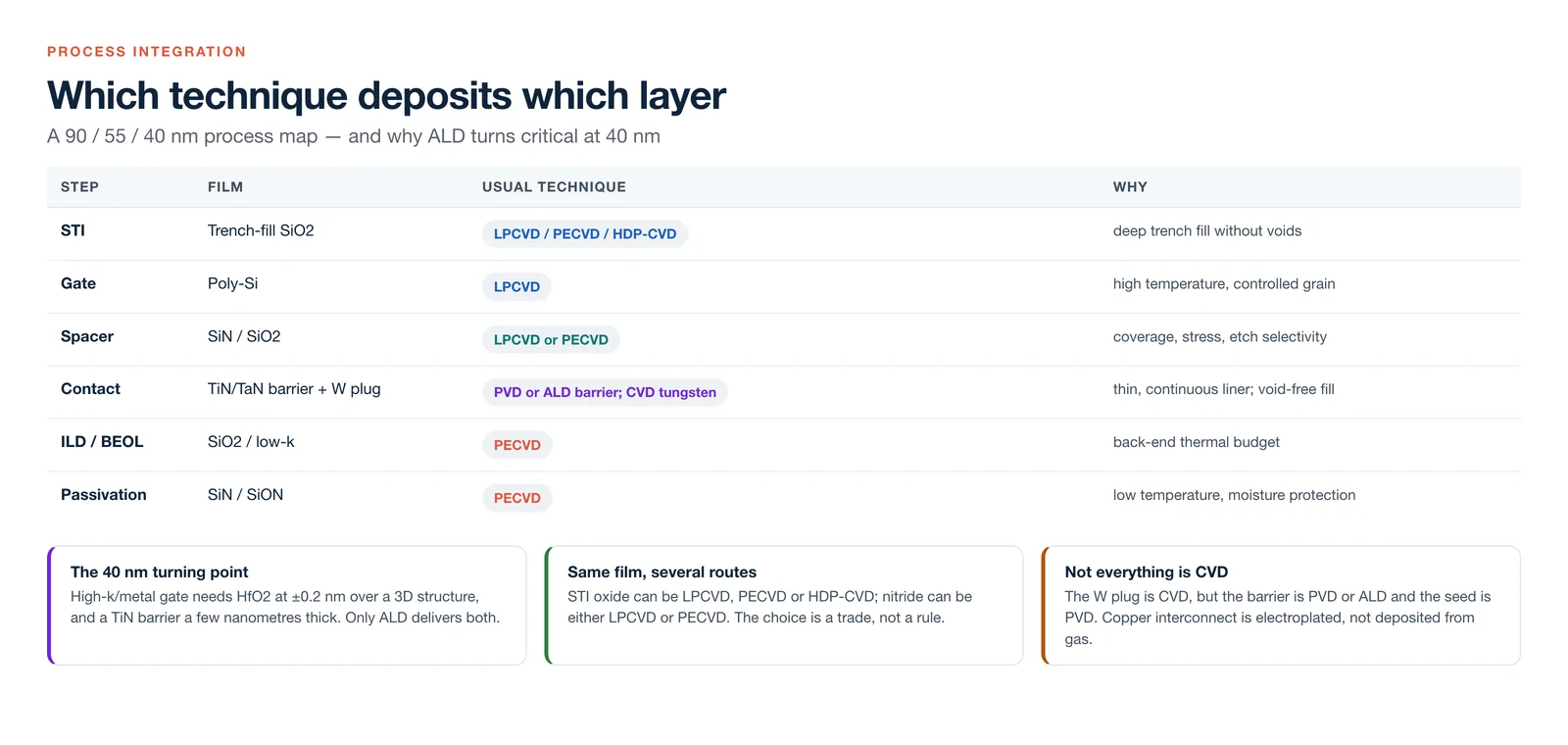
| STI | Trench-fill SiO₂ | LPCVD / PECVD / HDP-CVD | Deep trench fill without voids |
| Gate | Poly-Si | LPCVD | High temperature, quality, controlled grain |
| Spacer | SiN / SiO₂ | LPCVD or PECVD | Coverage, stress, etch selectivity |
| Contact | TiN/TaN barrier + W plug | PVD or ALD barrier; CVD tungsten | Thin, continuous barrier; void-free fill |
| ILD / BEOL | SiO₂ / low-k | PECVD | Back-end thermal budget |
| Passivation | SiN / SiON | PECVD | Low temperature, moisture and mechanical protection |
The shift from 55 nm to 40 nm is essentially the arrival of high-k/metal gate. At 55 nm, a polysilicon-plus-oxide stack with 2 nm or more of oxide has a comfortable process window. At 40 nm, HfO₂ a few nanometres thick with ±0.2 nm tolerance and uniform coverage over a three-dimensional structure is only achievable with ALD — and the same is true of the TiN/TaN barrier. That is the point at which ALD moves from marginal technique to key process.
Three things get confused in these discussions. The W plug is CVD, but the barrier is usually PVD or ALD and the seed is PVD — three different processes in one "contact". The interconnect metal itself is not CVD: aluminium is sputtered, copper is electroplated. And the same film can often be made several ways: STI oxide by LPCVD, PECVD or HDP-CVD; nitride by either LPCVD or PECVD. The choice is a trade between thermal budget, film quality, coverage and cost.
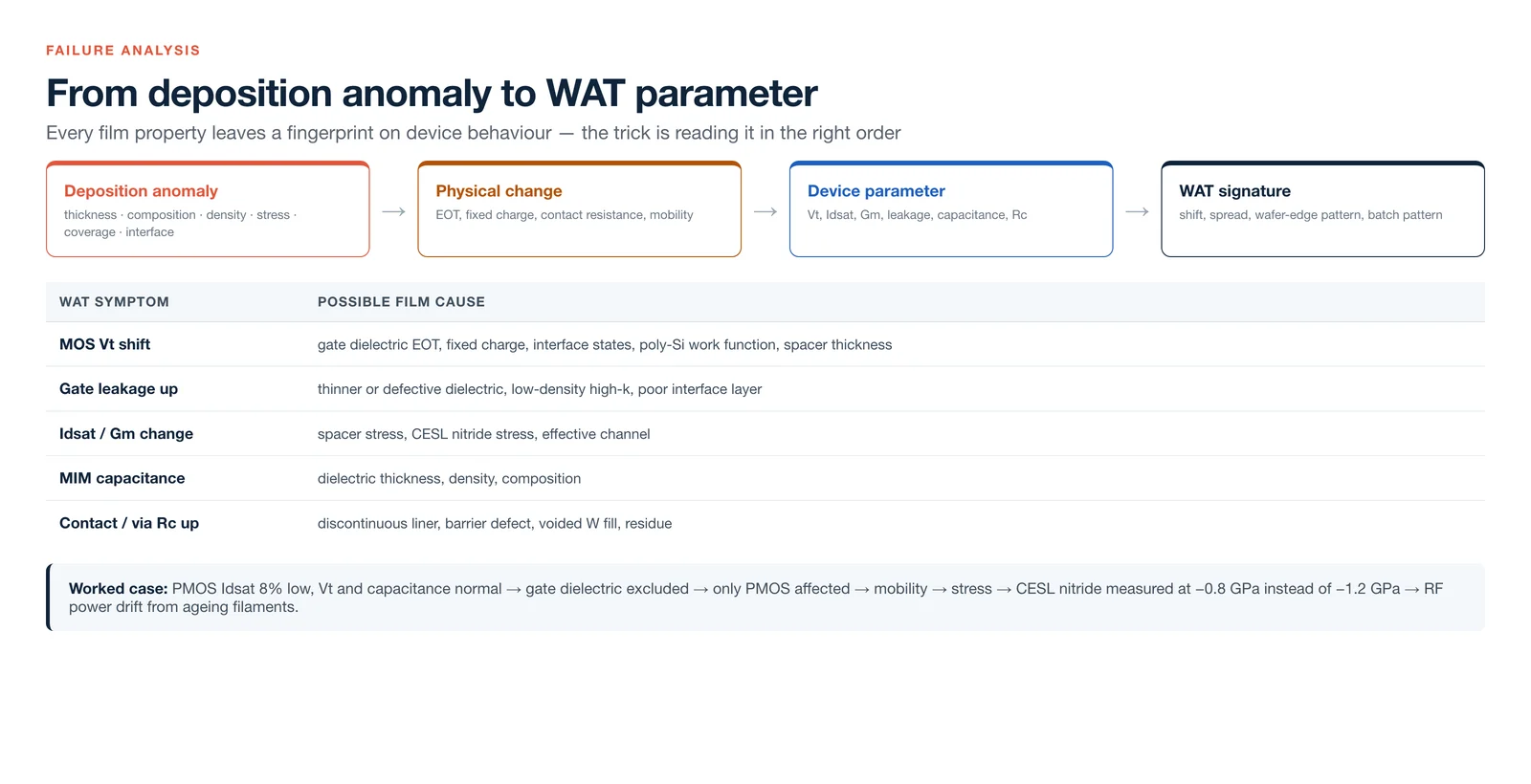
What deposition problems look like on WAT data
Deposition anomalies propagate in a predictable chain: physical change (thickness, density, stress, interface) → device parameter (EOT, mobility, contact resistance) → electrical test (WAT). Typical symptoms:
| WAT symptom | Possible film cause |
|---|---|
| MOS Vt shift | Gate dielectric thickness/EOT, fixed charge, interface states, poly-Si work function or doping, spacer thickness |
| Higher gate leakage | Thinner or defective gate dielectric, low-density high-k with impurities, poor interface layer |
| Idsat / Gm change | Spacer stress, CESL nitride stress, gate dielectric or poly-Si affecting the channel |
| MIM capacitance anomaly | MIM dielectric thickness, density/porosity, composition |
| High contact/via resistance | Discontinuous liner, barrier or metallisation problem, voided W fill, residue |
A real case: a batch showed PMOS Idsat about 8% low and Gm low, while Vt, NMOS, gate leakage and capacitance were all normal. Because Vt and capacitance were normal, the gate dielectric was excluded; because only PMOS was affected, the suspect was hole mobility. Mobility points at stress, and the film that supplies stress to a PMOS channel is the CESL nitride deposited by PECVD. Measured stress was −0.8 GPa against a −1.2 GPa target. Machine records showed a slow RF power drift from ageing filaments; lower power meant lower plasma density, more hydrogen and less compressive stress. Compensating the RF power restored Idsat to within ±2%.
The decision table
| Constraint | First choice | Reason |
|---|---|---|
| Throughput first, cost-sensitive, moderate thickness | APCVD | Fast, simple equipment, good for thick dielectric films |
| Film quality first, high temperature allowed (front end) | LPCVD | Dense, low defect, conformal, high batch throughput |
| Temperature-limited (back end) | PECVD | Plasma replaces heat; deposition at 150–450 °C |
| Ultrathin, high aspect ratio, perfect conformality | ALD | Self-limiting reaction, atomic thickness control |
Why this matters in solar cell manufacturing
The same four techniques, and the same trade-offs, decide how TOPCon and HJT cells are built. Polysilicon passivating contacts are formed by LPCVD (or PECVD) and then annealed at 600–700 °C — which is why TOPCon sits comfortably in a high-temperature process flow. Aluminium oxide passivation is deposited by ALD or PECVD, where the ALD route gives better interface quality at lower thickness. Silicon nitride anti-reflection and passivation layers are PECVD, because they must be deposited after metallisation and at low temperature.
For HJT the constraint tightens further: the amorphous-silicon passivation and transparent conductive oxide cannot survive much above 200 °C, so PECVD-based processes dominate the entire flow. That single thermal-budget constraint explains much of HJT's process complexity — and much of its capital cost.
Where deposition shows up in ZOEAST PV's supply chain
ZOEAST PV's n-type cells come off 5 GW of TOPCon capacity in Yixing, where the stack described above is built with LPCVD polysilicon, PECVD silicon nitride and aluminium oxide passivation deposited by ALD or PECVD. When we qualify a new cell line, we look at the deposition sequence — which tool, which thermal budget, which passivation stack — before we look at the nameplate efficiency.
The reason is commercial rather than academic: two cells rated at the same wattage can differ in degradation, PID behaviour and damp-heat performance depending on how those films were deposited and annealed. For HJT-based products the 200 °C ceiling reshapes the whole flow, and for BC cells the same constraint shows up as bowing after stringing.
Specifications for the cells we supply are on the solar cell page; for a technical comparison of a manufacturing or procurement decision, talk to our engineering team.
Figures: ZOEAST PV, redrawn in English from the original technical article.